Breakthrough in 2D Material Transistor Integration at 300 mm Scale
At the 2026 IEEE/JSAP Symposium on VLSI Technology and Circuits, imec, a global leader in advanced semiconductor research, together with ASML and TSMC, unveiled a pioneering 300 mm integration process for 2D-material-based nFETs and pFETs. This collaboration marks the first successful demonstration of scaled nFETs using molybdenum disulfide (MoS2) and pFETs based on either tungsten disulfide (WS2) or tungsten diselenide (WSe2) with a 50 nm contacted poly pitch (CPP). These devices exhibit strong current-voltage characteristics, representing a significant milestone in transitioning 2D-material transistors from laboratory research to industrial fabrication for ultra-scaled logic and advanced back-end applications.
Advancing Logic Scaling with 2D Transition Metal Dichalcogenides
Two-dimensional transition metal dichalcogenides (TMDs) such as MoS2, WS2, and WSe2 are emerging as promising alternatives to silicon for next-generation transistors. Their atomically thin structure enables excellent electrostatic control and maintains favorable carrier mobility, even at extremely scaled gate and channel lengths. This makes TMDs highly attractive for ultra-scaled logic, back-end-of-line, and wafer backside applications.
Despite their potential, industrial adoption of TMD-based transistors has been limited by the absence of a robust 300 mm integration route that delivers both n-type and p-type FETs at industry-relevant dimensions without sacrificing performance. The joint efforts of imec, ASML, and TSMC have now resulted in a scalable, back-end-compatible 300 mm process for TMD-based nFETs and pFETs, achieving several key breakthroughs:
- First-ever demonstration of scaled nFETs and pFETs with a 50 nm contacted poly pitch (CPP)
- Very low off-state current (Ioff) at zero gate voltage for both transistor types
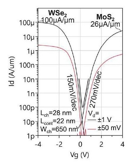
- WSe2-based pFETs performing close to record-setting lab devices
The integration approach, which enables both nFETs and pFETs on the same 300 mm wafer, achieved a 94% operational yield (Imax/Imin > 105), demonstrating its robustness and stability. Importantly, the process flow is adaptable to other 2D channel materials beyond MoS2, WS2, and WSe2.
Enabling Ultra-Scaled Transistors with Advanced Lithography
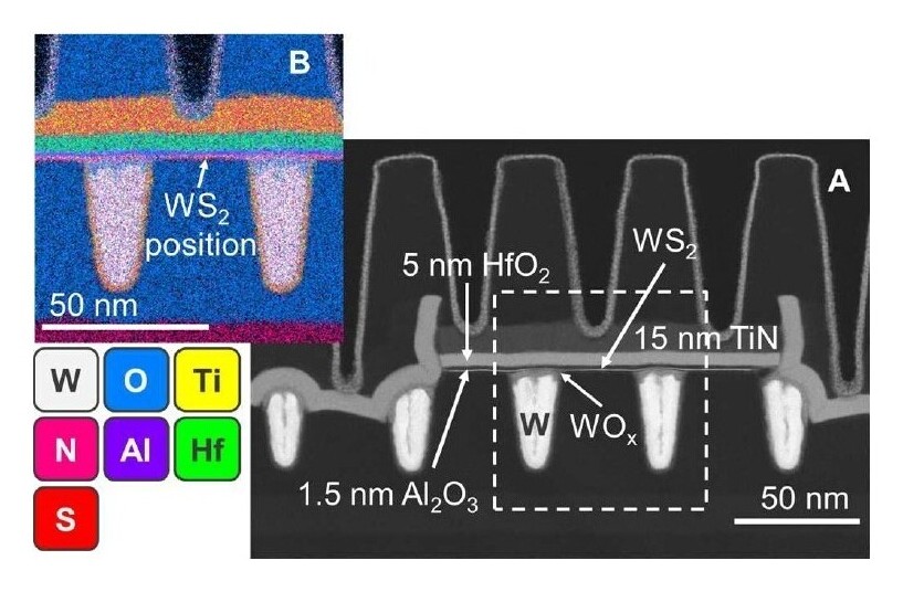
According to Gouri Sankar Kar, VP of R&D for compute and memory device technologies at imec, "Transistors based on 2D TMD materials are typically optimized for small channel lengths, but often require large contact areas to minimize resistance, which limits further scaling. For the first time, we achieved a 50 nm CPP—a metric defined by both gate length and source/drain contact length—without compromising the performance of 2D nFETs and pFETs. This was made possible by leveraging single-patterning extreme ultraviolet (EUV) lithography, developed in close collaboration with ASML."
The resulting transistors display excellent current-voltage behavior, with pFETs nearly matching the best lab-based devices—a significant achievement for TMD technology. Both nFETs and pFETs reliably switch off at zero gate voltage, a result attributed to an innovative "reverse" thin-film transistor (TFT) fabrication flow. Unlike conventional 2D transistors, this approach uses bottom contacts and an overlapping deposited gate, realized by transferring the TMD channel material onto pre-patterned tungsten-filled trenches that serve as contacts.
Accelerating the Lab-to-Fab Transition
Dr. Min Cao, Vice President and CTO at TSMC, emphasized the strategic value of this collaboration: "Our research partnership is crucial for advancing semiconductor innovation. By focusing on de-risking and accelerating the lab-to-fab transition, we ensure that breakthroughs in novel channel materials can be efficiently integrated into advanced manufacturing, delivering state-of-the-art solutions."
"2D TMD materials could potentially enable much smaller and higher-performance transistors than those based on silicon, but 2D-channel devices that have been demonstrated so far using 300 mm processes are actually fairly large, and patterned using older lithographic technologies. Thanks to the much sharper resolution of EUV lithography, we were able to create TMD transistors with channel lengths as small as 28 nm, and at a pitch compatible with the most advanced transistor nodes."
— Etienne De Poortere, Director Technology Development Center Europe, ASML
This achievement marks a pivotal step toward the industrialization of 2D-material-based transistors, paving the way for future generations of ultra-scaled, high-performance semiconductor devices.